Profession
易于使用的集成“即插即用”配置用于前照灯系统
当前位置:首页 > Products > Profession > UV LED >
Learn how UV applications can be implemented to provide new light sources for industrial curing, sterilization/disinfection, etc.
MORE>
UA275-35F 0.3W/3535 Product introduction
The LED uses our glass lens + high-power 3D ceramic packaging technology + UVC LED chip, with UVC wavelength range of 270-280nm.
UA275-35F 0.3W/3535 Product advantages
3535 ceramic packaging is compatible with many different type of standard PCB board
UVC LED has high irradiance and optical power output
Primary optical lens emission design with 120° light angle
Excellent reliability, high performance at low cost
Product features
High-power 3D-ceramics package, Glass LENS
UVC ultraviolet radiation , Korean UVC LED chip
Size: 3.5mmx3.5mmx1.6mm
Zener protection
Solder method: SMT
Product Showcase
Electro Characteristics: (T solder pad =25℃,IF=40mA) |
Product | Peakwavelength (nm) | Total Rad Flux (mW) | Voltage (V) | Directivity 2θ1/2 (degree) | Current (mA) |
Typ. | Max. |
UA275-35F (Glass LENS) | 270-280 | 2-5 | 6.8 | 8.0 | 120° | 40 |
applications
UVC surface sterilization
Portable sterilization scheme
Biochemical analysis
Reference
UB275-35F 0.3W/3535 Product introduction
The LED uses our glass lens + high-power 3D ceramic packaging technology + UVC LED chip, with UVC wavelength range of 270-280nm.
UB275-35F 0.3W/3535 Product advantages
3535 ceramic packaging is compatible with many different type of standard PCB board
UVC LED has high irradiance and optical power output
Primary optical lens emission design with 120° light angle
Excellent reliability, high performance at low cost
Product features
High-power 3D-ceramics package, Glass LENS
UVC ultraviolet radiation , Korean UVC LED chip
Size: 3.5mmx3.5mmx1.6mm
Zener protection
Solder method: SMT
Product Showcase
Electro Characteristics: (T solder pad =25℃,IF=40mA) |
Product | Peakwavelength (nm) | Total Rad Flux (mW) | Voltage (V) | Directivity 2θ1/2 (degree) | Current (mA) |
Typ. | Max. |
UB275-35F (Glass LENS) | 270-280 | 7-15 | 5.0 | 8.0 | 120° | 100 |
applications
UVC surface sterilization
Portable sterilization scheme
Biochemical analysis
Reference
VD 2W/3535 Product introduction
The LED uses our GaN-on-Si UVA chips and 3535 high-power ceramic packaging process,with wavelength range of 365~375nm and 390~400nm.
VD 2W/3535 Product advantages
3535 ceramic packaging is compatible with many different type of standard PCB board
UVA LED has high irradiance and optical power output
Primary optical lens emission design with 120° light angle
Excellent reliability, high performance at low cost
Product features
High-power ceramics package, High radiant energy
Si-UV LED chip
Size: 3.5mmx3.5mmx2.3mm
8KV electrostatic protection
Solder method: SMT
Product Showcase
| Electro Characteristics (T solder pad =25 ℃) |
| Product | Peak Wavelength (nm) | Total Rad Flux (mW) | Voltage(V) | Directivity 2θ1/2 (degree) | Electric current (mA) |
| Typ. | Max. |
VD
(VDC6W) | 395 (390-400nm) | 500-800 | 3.3 | 3.8 | 120° | 350 |
369 (365-375nm) | 400-700 | 3.5 | 4.0 | 120° | 350 |
applications
Purple color
Plant lighting
Fluoresce detection
Photocatalyst
Reference
VE 3W/3535 Product introduction
The LED uses our GaN-on-Si UVA chips and 3535 high-power ceramic packaging process,with wavelength range of 370nm/385nm/395nm/405nm.
VE 3W/3535 Product advantages
3535 ceramic packaging is compatible with many different type of standard PCB board
UVA LED has high irradiance and optical power output
Primary optical lens emission design with 120° light angle
Excellent reliability, high performance at low cost
Product features
High-power ceramics package, high radiant energy
Si-UV LED chip
Size: 3.5mmx3.5mmx2.3mm
8KV electrostatic protection
Solder method: SMT
Product Showcase
Electro Characteristics: (T solder pad =25 ℃,IF=500mA) |
Product | Peakwavelength (nm) | Total Rad Flux (mW) | Voltage (V) | Directivity 2θ1/2 (degree) | Current (mA) |
Typ. | Max. |
VE-G | 405 (400-405) | 800-1100 | 3.45 | 3.8 | 120° | 500 |
395 (390-400) | 800-1100 | 3.45 | 3.8 | 120° | 500 |
385 (380-390) | 800-1100 | 3.45 | 3.8 | 120° | 500 |
370 (365-375) | 700-1000 | 3.6 | 4 | 120° | 500 |
applications
Industrial curing
Acteriostatic
Exposure
Reference
VS 3W/3535 Product introduction
The LED uses our GaN-on-Si UVA chips and 3535 high-power ceramic packaging process,with wavelength range of 370nm/385nm/395nm/405nm.
VS 3W/3535 Product advantages
3535 ceramic packaging is compatible with many different type of standard PCB board
UVA LED has high irradiance and optical power output
Primary optical lens emission design with 55° light angle
Excellent reliability,high performance at low cost
Product features
High-power ceramics package, high radiant energy
Si-UV LED chip
Size: 3.5x3.5mmx3.1mm
8KV electrostatic protection
Solder method: SMT
Product Showcase
Electro Characteristics :(T solder pad =25 ℃,IF=500mA) |
Product | Peakwavelength (nm) | Total Rad Flux (mW) | Voltage (V) | Directivity 2θ1/2(degree) | Current (mA) |
Typ. | Max. |
VS-G | 405 (400-405) | 800-1100 | 3.45 | 3.8 | 55° | 500 |
395 (390-400) | 800-1100 | 3.45 | 3.8 | 55° | 500 |
385 (380-390) | 800-1100 | 3.45 | 3.8 | 55° | 500 |
370 (365-375) | 700-1000 | 3.6 | 4 | 55° | 500 |
applications
Industrial curing
Bacteriostasis
Exposure
Reference
VG 3W/3838 Product introduction
The LED uses our GaN-on-Si UVA chips and 3838 high-power ceramic packaging process, with wavelength range of 380-390nm & 390-400nm.
VG 3W/3838 Product advantages
3838 ceramic packaging is compatible with many different type of standard PCB board
UVA LED has high irradiance and optical power output
Primary optical lens emission design with 50° light angle
Excellent reliability, high performance at low cost
Product features
High-power 3D-ceramics package,glass LENS,high radiant energy
Si-UVLED chip
Size: 3.85mmx3.85mmx3.31mm
8KV electrostatic protection
Solder method: SMT
Product Showcase
Electro Characteristics: (T solder pad =25 ℃,IF=650mA) |
Product | Peakwavelength (nm) | Total Rad Flux (mW) | Voltage(V) | Directivity 2θ1/2(degree) | Current (mA) |
Typ. | Max. |
VG-G6E (Glass Lens) | 395 (390-400) | 1000-1300 | 3.5 | 3.8 | 50° | 650 |
385 (380-390) | 1000-1300 | 3.5 | 3.8 | 50° | 650 |
UVC Air Modules Product introduction
This UVC module for air sterilization uses 270-280nm UVC chip imported from South Korea and uses special aluminum substrate plus high-precision packaging to realize low thermal resistance, strong heat dissipation and high reliability. At the same time, it achieves high-density UV light output in a small luminous area and sterilization rate up to 99.99% to meet the requirements of sterilization and other applications.
UVC Air Modules Product advantages
The LED is made of UVC chip 270-280nm, with high sterilization efficiency, up to 99.99%
Imported chip from South Korea with high reliability
Low thermal resistance and strong heat dissipation ability of PCB customized aluminum plate
Product features
Size : 110*12*1 mm (Customizable)
Special Al substrate with high precision packaging combined to reach high stability
Product Showcase
Electro Characteristics: (T solder pad =25 ℃) |
Peak Wavelength (nm) | Radiation Power (mW) | Viewing Angle | Forward Voltage (V) | Power (W) |
Typ.@40mA |
270~280 | 6-15 | 120° | 15-24 | 0.84 |
applications
Car sterilization
Daily life sterilization
Medical sterilization
Reference
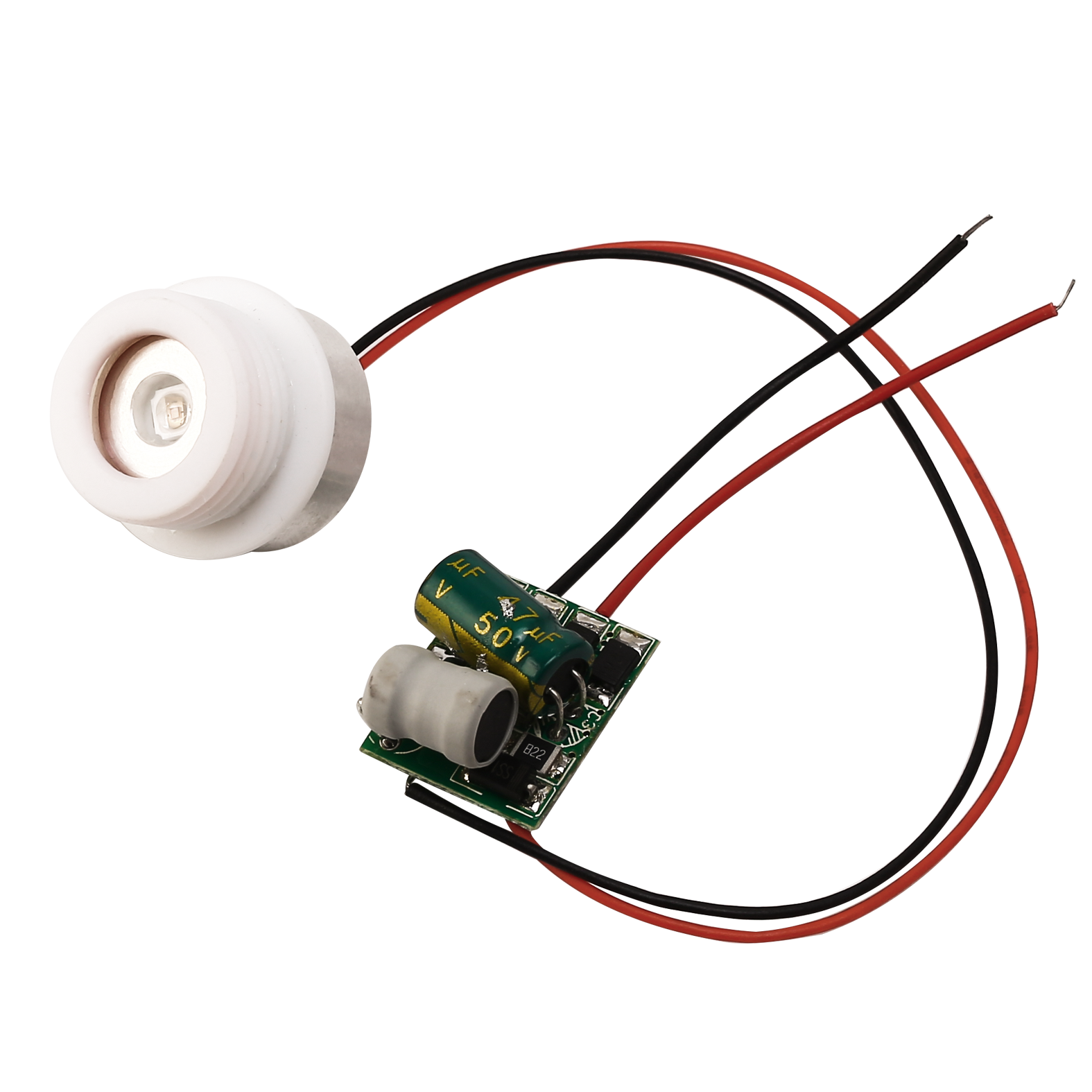
UVC Water Modules Product introduction
SW4.1A module for static water sterilization has small size ,high conversion rate and high output power , and can effectively kill germs and virus with 275 nm LEDs which can meet main applications of static water sterilization in water dispenser, coffee machine, humidifier, etc.
UVC Water Modules Product advantages
It has highefficiency optical power output and can reach 3mW outputpower under 50mA
It has wide voltage input with 9-36V DC adaptive and can control operation tempreture of module
It has long lifetime that L80 can be up to 3000h
Product features
Small size with diameter of 16.6mm(G3/8 external thread) and length of 16mm to enable more products design.
It meets the requirement of enviroment and all the national and international standard related water matierals.
Product Showcase
Electro Characteristics : ( T solder pad =25 ℃ ) |
Peak Wavelength (nm)
| Radiation Power (mW) | Viewing Angle | Forward Voltage (V) | Power (W) |
Typ.@40mA |
270~280 | 2-5 | 120° | 5-8 | 0.28 |
applications
Water purification equipment
Maternal and child products
Coffee machine humidifier
Brewing machine
Water dispenser
Sterilization cup,etc
Reference
Photocatalyst Modules 40 Series Product introduction
The 40 series of photocatalyst product uses silicon based UVA LEDs and nano-Photocatalyst particles to realize better air purification effect.
Photocatalyst Modules 40 Series Product advantages
It can activate TiO2 effectively with 375nm LEDs to kill germs and eliminate harmful gases
Phototalalyst with robust attachment has good stability,large reaction area,good stability and high efficiency
The module has the advantages of small size and long lifetime,can be operated in people friendly environment
Product features
UV LED is 0.5W/1W
Electric power 1~4W, Voltage 5V/12V, light power 400-600mW
Module size :40*40*(16~40)mm
Product Showcase
Electro Characteristics: (T solder pad =25 ℃) |
Product | LED | Carrier | Wavelength (nm) | Total Rad Flux (mW) | Voltage (V) | Directivity 2θ1/2(degree) | Current (mA) |
40 Series | EU-A | Ceramics | 365-375 | 400~1600 | 12 | 90° | 100~600 |
VD-Y | Ceramics | 365-375 | 450~900 | 5 | 120° | 300~700 |
applications
Refrigerator
Cat litter box
Shoe cabinet, etc
Reference
Photocatalyst Modules 50 Series Product introduction
The 50 series of photocatalyst uses silicon based UVA LEDs and nano-Photocatalyst combined to achieve better air purification effect.
Photocatalyst Modules 50 Series Product advantages
It can activate TiO2 effectively with 375nm LEDs to kill germs and eliminate harmful gases
Phototalalyst with robust attachment has good stability,large reaction area, good stability and high efficiency
The module has the advantages of small size and long lifetime,can be operated in people friendly environment
Product features
UV LED is 0.5W/1W
Electric power 3~8W, Voltage 12V, light power 1200-3500mW
Module size :50*50*(18~44)mm
Product Showcase
| Electro Characteristics (T solder pad =25 ℃) |
Product | LED | Carrier | Wavelength (nm) | Total Rad Flux (mW) | Voltage (V) | Directivity 2θ1/2(degree) | Current (mA) |
50 Series | EU-A (EMC) | Ceramics | 365-375nm | 1600~3500 | 12 | 90° | 400~1000 |
VD-Y (Ceramics) | Ceramics | 365-375nm | 1200~2500 | 12 | 120° | 300~700 |


