LatticePower: Industrialization Path of GaN based Micro LED on Large Silicon Substrate
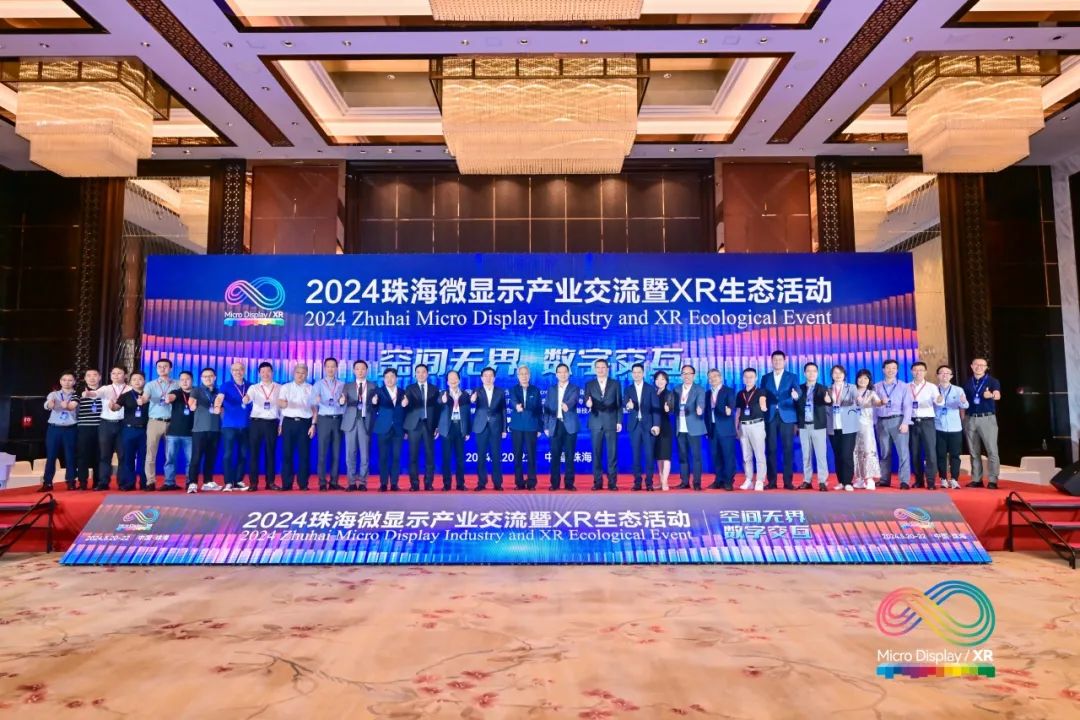
From May 20th to 22nd, the 2024 Micro Display Industry Exchange and XR Ecological Activity with the theme of "Boundless Space, Digital Interaction" was grandly held in Zhuhai.
This event presented a high-level forum led by top academicians, covering three major technical fields, with over 30 high-level corporate guests and 50+core topics. It also gathered several well-known companies in the industry chain.
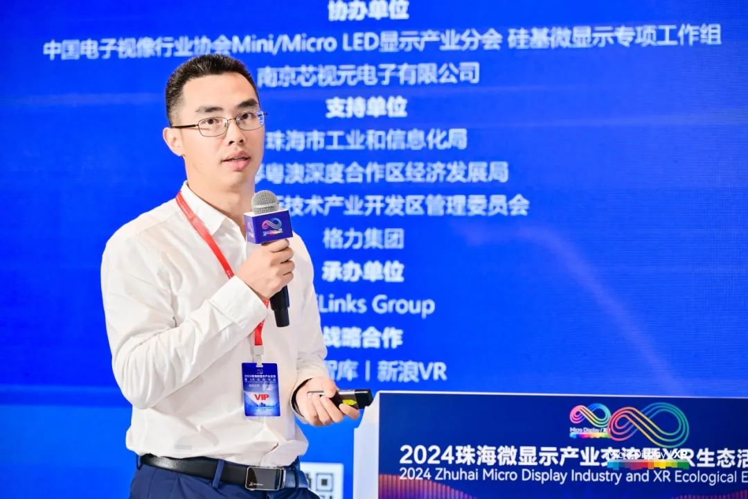
Zhou Mingbing, Senior Manager of Crystal Energy Optoelectronic Epitaxy Technology, was invited to attend the event with "Industrialization Road of GaN based Micro LED on Large Silicon Substrate", and shared the application overview of GaN material on silicon substrate in the field of optoelectronics, the development of GaN based Micro LED on large silicon substrate, and the current development status of Crystal Energy Optoelectronic Large scale Epitaxy.
Application of GaN material on silicon substrate in the field of optoelectronics
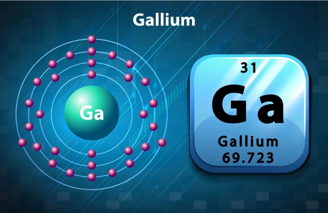
GaN (Gallium Nitride) is a third-generation semiconductor material that can be used to prepare semiconductor lasers, RF PAs, power HEMTs, lighting LEDs, Micro LEDs, etc. based on different substrates, growth techniques, and epitaxial structures, with broad application prospects.
Silicon based GaN materials have the advantage of large substrate prices, which can fully utilize integrated circuit processes and equipment to achieve high efficiency, high yield, low-cost precision device manufacturing processes, and have the potential advantage of highly functional integration with CMOS backplanes. But before entering industrialization, breakthroughs must be made in key indicators such as material quality, material uniformity, appearance defects, and wafer warping, which mainly come from the high defect density caused by lattice mismatch between silicon substrate and GaN, tensile stress caused by thermal expansion coefficient mismatch, and Ga: Si reaction.

At present, silicon based GaN materials have achieved large-scale applications in the fields of low to medium power high-frequency HEMTs and LED professional lighting. At the same time, with the rapid development of AR/VR, car HUD, matrix headlights, smart wearables, optical communication and other fields, Micro LED micro display technology and low-power PA based on silicon based GaN materials are accelerating their engineering development. DUV LED, GaN LD and GaN/CMOS integrated architectures are also in early research.
Development of GaN based Micro LEDs on large-sized silicon substrates
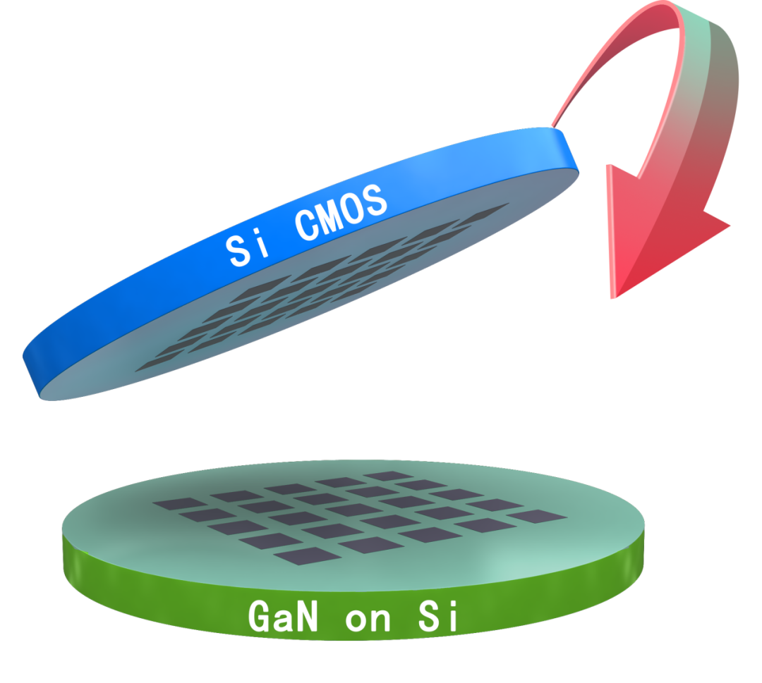
The main application scenarios of large-sized GaN based Micro LEDs on silicon substrates are high PPI projection directly bonded to CMOS substrates, and near eye display for auxiliary/virtual reality devices. It is based on GaN on Si wafers of 8 inches or more and CMOS substrates, and draws on mature IC processes. Its advantages include large size, low cost, high wavelength consistency, non-destructive removal, low warpage, CMOS compatibility, etc., which can effectively improve process efficiency and yield, and reduce manufacturing costs.
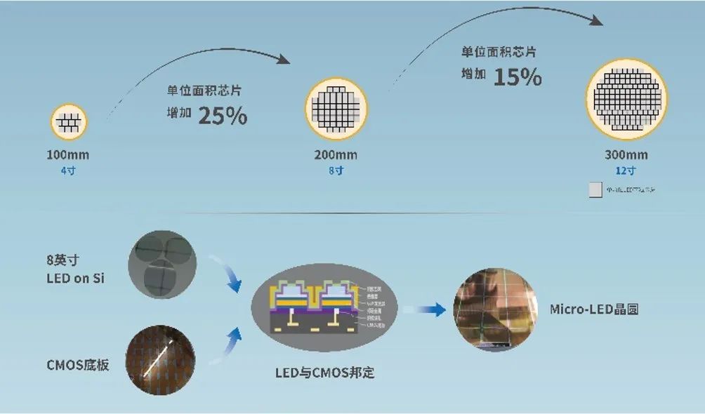
Therefore, the development of Micro LED chips will transition from 4-inch process research and development to 8-inch mass production, and ultimately upgrade to 12 inch wafer process. Many start-ups at home and abroad are focusing on the development of Micro LED technology based on silicon substrate GaN, and major consumer electronics companies in China, the United States, Japan, South Korea, and other countries are also actively laying out in this emerging field.
Development Status of GaN Epitaxy on Large scale Silicon Substrate for Crystal Energy Optoelectronics
In order to obtain high-quality GaN epitaxial growth on silicon substrates, the company adopts a stress accumulation and release model of heteroepitaxy to optimize growth, innovatively utilizing lattice stress-induced dislocation reactions. Under the condition of a total epitaxial layer thickness of 5 μ m, the company can stably and repeatedly grow GaN epitaxial layers on silicon substrates with a dislocation density of~1.5E8/cm2; At the same time, using thin buffer technology, GaN epitaxy with a thickness exceeding 8 μ m was obtained, and the film thickness uniformity was good.
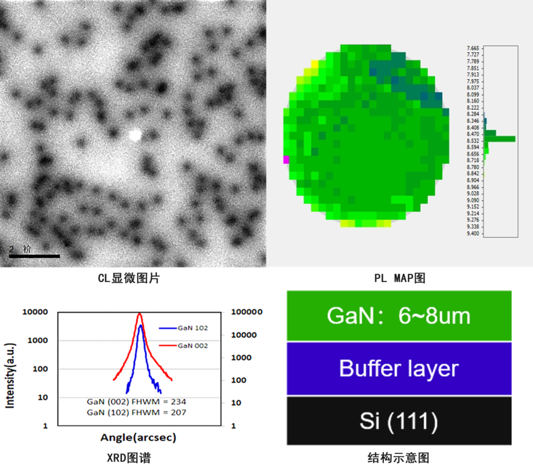
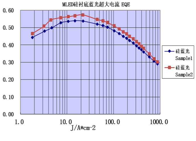
At present, LatticePower has the 365-650nm full-color silicon substrate GaN LED epitaxial technology, and has developed 4-12-inch silicon substrate GaN based red/green/blue Micro LED epitaxy, which can provide high-quality epitaxial wafers with standard thickness product grade 8-inch CMOS matching. The peak external quantum efficiencies of the high-power vertical LED chips with blue and green silicon substrates mass-produced by the company have reached over 85% and 50%, respectively, and are widely used in fields such as automotive lighting, mobile lighting, and consumer electronics.
At present, red LED is still one of the major bottlenecks in Micro LED technology, and AlGaInP has the problem of low efficiency. GaN based red LED can achieve a full GaN system, while driving design has consistency. However, GaN red light has high efficiency FWHM、 There are still significant challenges in wavelength drift and other aspects, but with extensive development investment from industry, academia, and research, there are constantly new directions and process equipment upgrades, and it is expected that there will be sustained breakthroughs.
Looking towards the future, the potential areas of silicon substrate GaN technology lie in large-size, highly integrated, and miniaturized processes. Micro LED displays are also expected to become a major market opportunity for silicon substrate GaN technology. LatticePower focuses on the development of silicon substrate GaN LED materials and hopes to cooperate with upstream and downstream enterprises in the industry on Micro LED applications to jointly promote the development of the industry.


